|
|
This article was published in Danish, in the Danish radio armature magazine "OZ" in November 2009
|
|
25W + 150W 70 MHz PA.
By Thomas Gosvig OZ1JTE, Denmark..
|
|
|
The need of power.
Suddenly one day I got my old 50 MHz OE9PMJ transverter back from a friend who had borrowed the transverter some years ago.
|
|
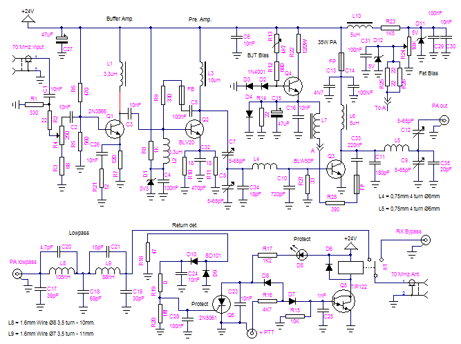
Fig 9 Schematic of the first 25 W amplifier, directional coupler and low pass filter.
|
|
|
|
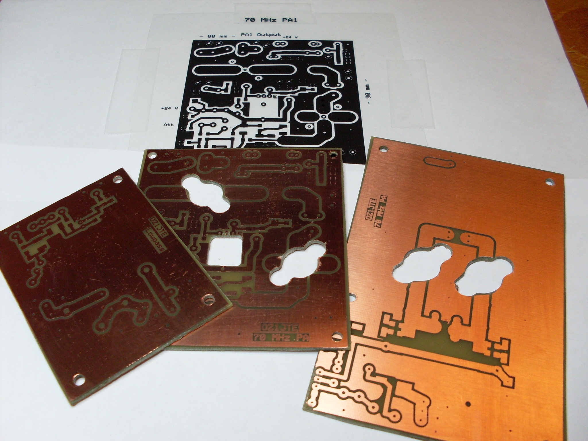
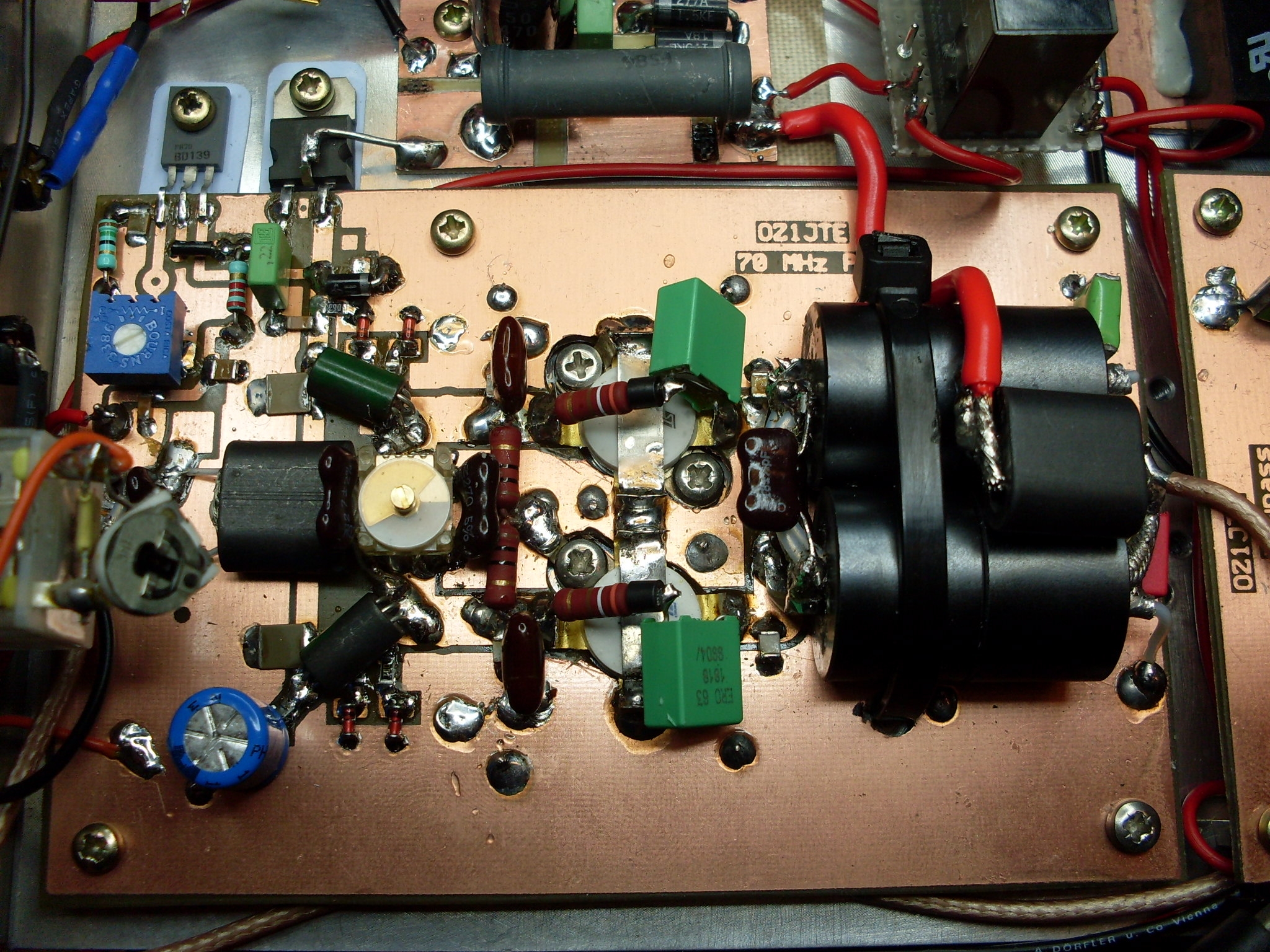
Fig 2 PCB ready for soldering |
Fig 6 Low pass filter |
The first 25 W was made by 3 stages. A 2N3866 that should give the first boost to feed a BLV20, and from there feed a BLW50F that should give the final gain.
The BLW50F is a 48 V transistor, but because I earlier had managed to get good results on lower voltages, I decided to use this device.(Ref. 1)
Later it showed that it was easily to realize the goal of 25 W output. Fig. 9 shows the schematic.
Because the very close association between IMD3 in the fist stages in a power amplifier and the final IMD3 at the output, I was able to insure the final IMD3 and linearity would be satisfying when I designed the 2 first stages as class A amplifiers. Even at the last stage there will be room to raise the bias a bit also to insure the linearity.
This "3 stage rocket" can be used after most of the known lowpower transverters, and as I found later on, feeding this board with a input of 100 mW, power output close to 35 W at 24 V was no problem to obtain.
My attenuator was adjusted for 24 dB of gain, and this ensured 25 W of output.
After this you could place the low pass filter and use the system as it is.
But if you are a little bit more ambitious you also could go for the next step;.
|
|
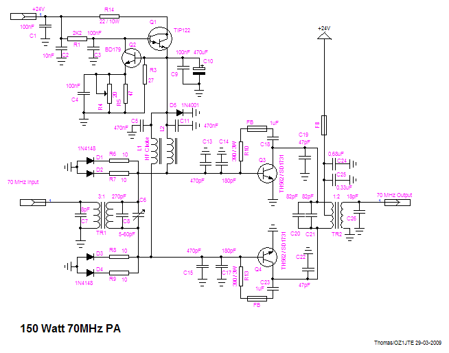
Fig 10 Schematic 150W output PA
|
|
|
|
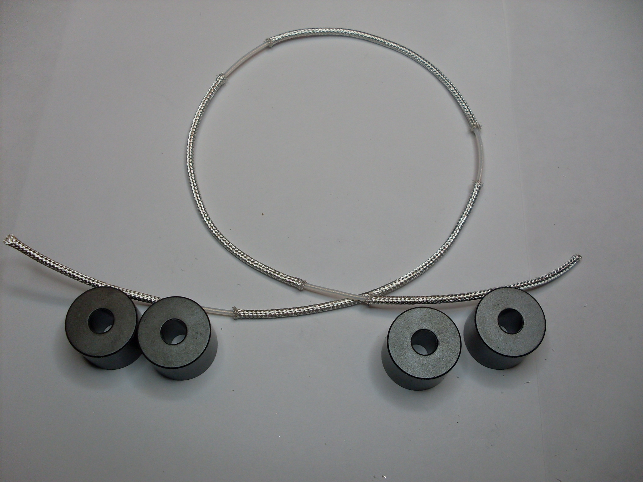
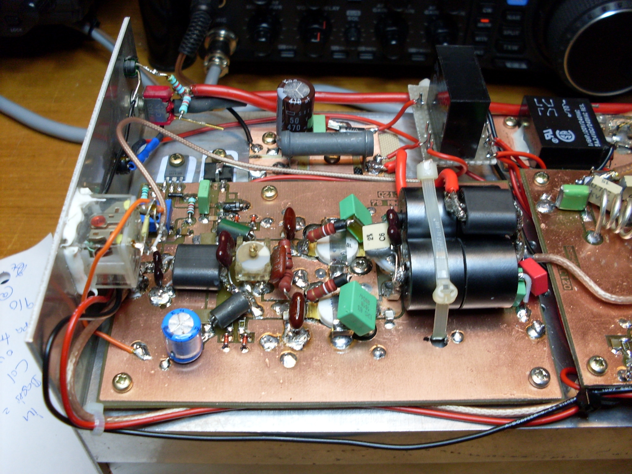
Fig. 5 Ready for output transformer |
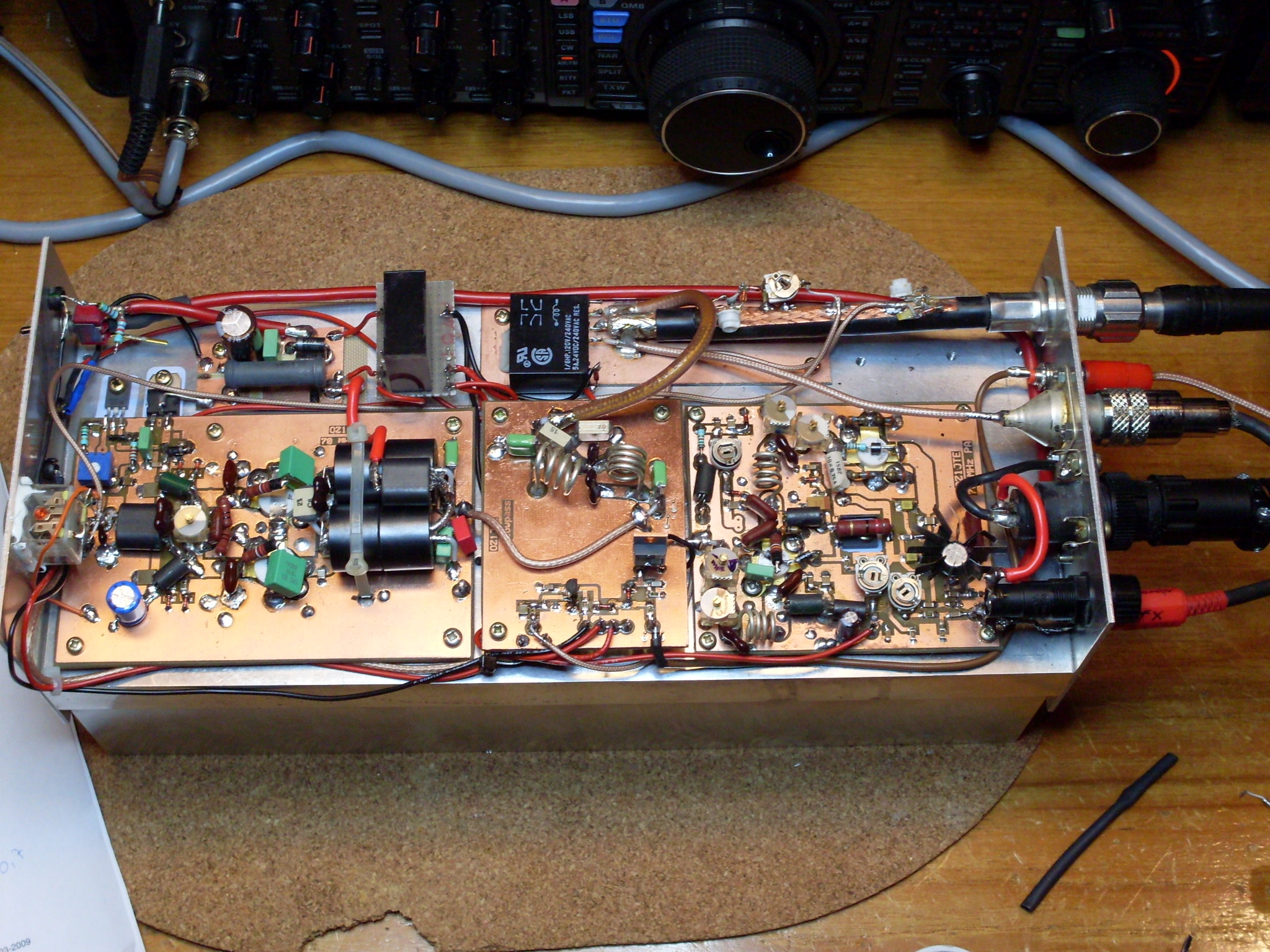
Fig 3 First PA and directional coupler |
Step 2.
Maybe you don't feel that 25 Watts is enough for your wish, so if you want a little more then you could use the next step to achieve your goal.
This idea will increase the output to 120 Watt.
This Power Amplifier is made of a traditional push-pull design that will raise the input approximately 7 dB.
At this design I use 2 pieces of 48 V transistors but again I only use the devices at 24 V.
This will ensure a stable and a robust stage, although you will have less gain at this lower operating voltage.
The schematic is found at Fig 10.
The device name is SD1731 or TH562.
I use a bias of about 200 mA (400 mA for both devices) and this will ensure a good linearity and operation in class AB.
I am sure that many other types of transistors could be used as a replacement in this design, only causing minor modifications.
Maybe the "open" 3:1 input transformer is not the very best transformer type at 70 MHz, but I did't felt to concern about a little loss here at the input stage.
The wounding of the transformer is done the traditional HF technique way. 3 primary windings is made inside a single secoundary outer winding consisting of a piece of shielding from a multi wire cable. I have used a binocular ferrit core.
As I already mention I was not concerned about the loss in the input transformer, but in the output transformer I tried to minimize the loss. This transformer is a 1:2.
I chose to use RG-316 coaxial cable for this transformer. This will ensure low leakage and better high frequency specifications.
Again maybe not the perfect transformer type at this frequency, but a test using 2 transformers "back to back" revealed only a minor loss and therefore I selected this type of transformer. The test showed 1 dB of loss. 0.5 dB of loss at each transformer. Of cause it is very important that the transformer is compensated using capacitors at the input and output of the transformes in the final design.(Litt. 2).
The ferrite I used has a permeability around 100, and of cause I use a size that will handle the power. Check also the part list. At Fig. 5 you see how the RG-316 is made ready for the winding of the transformer. After the winding the cable shield is soldered together.
|
|
|
|
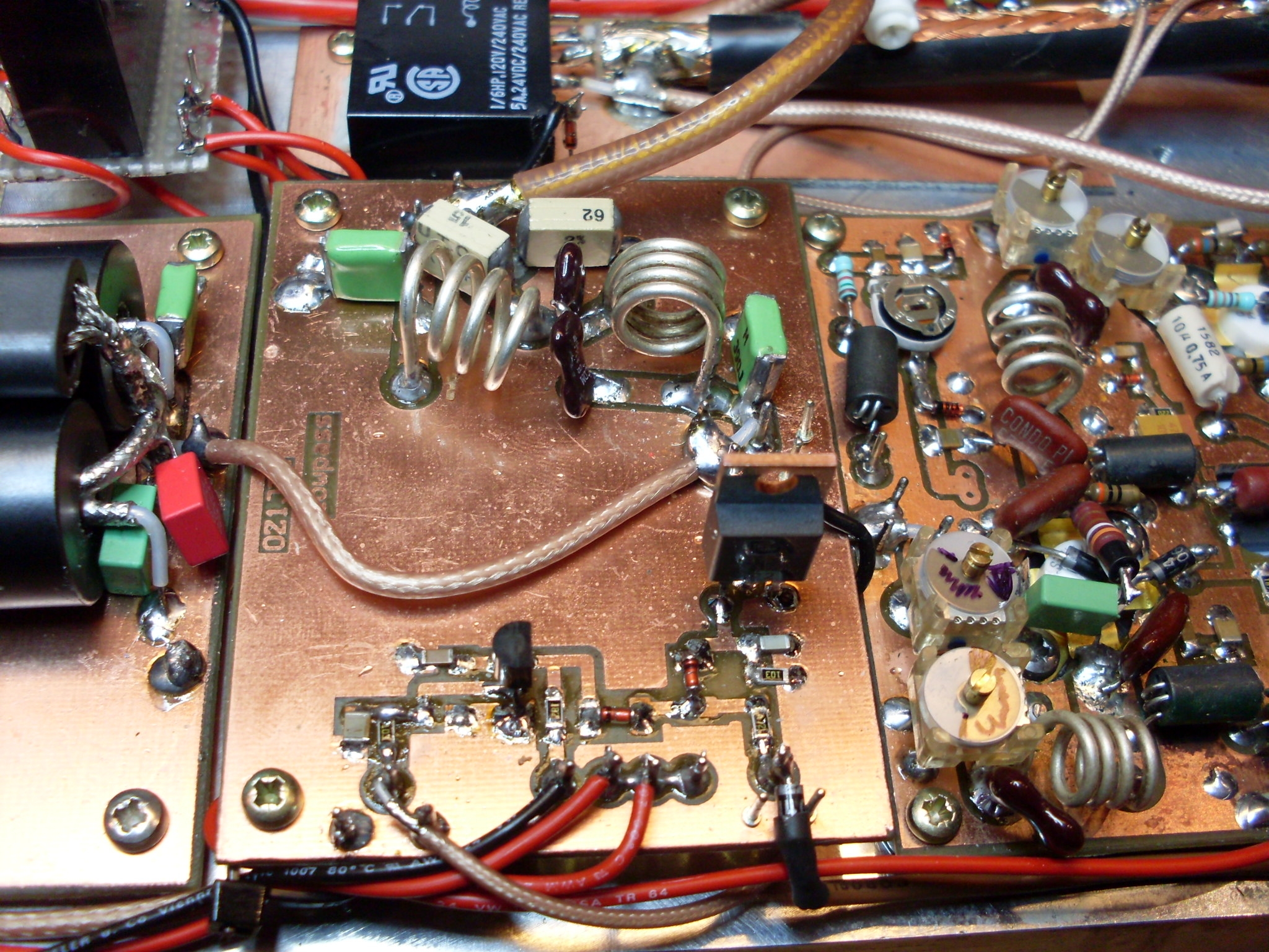
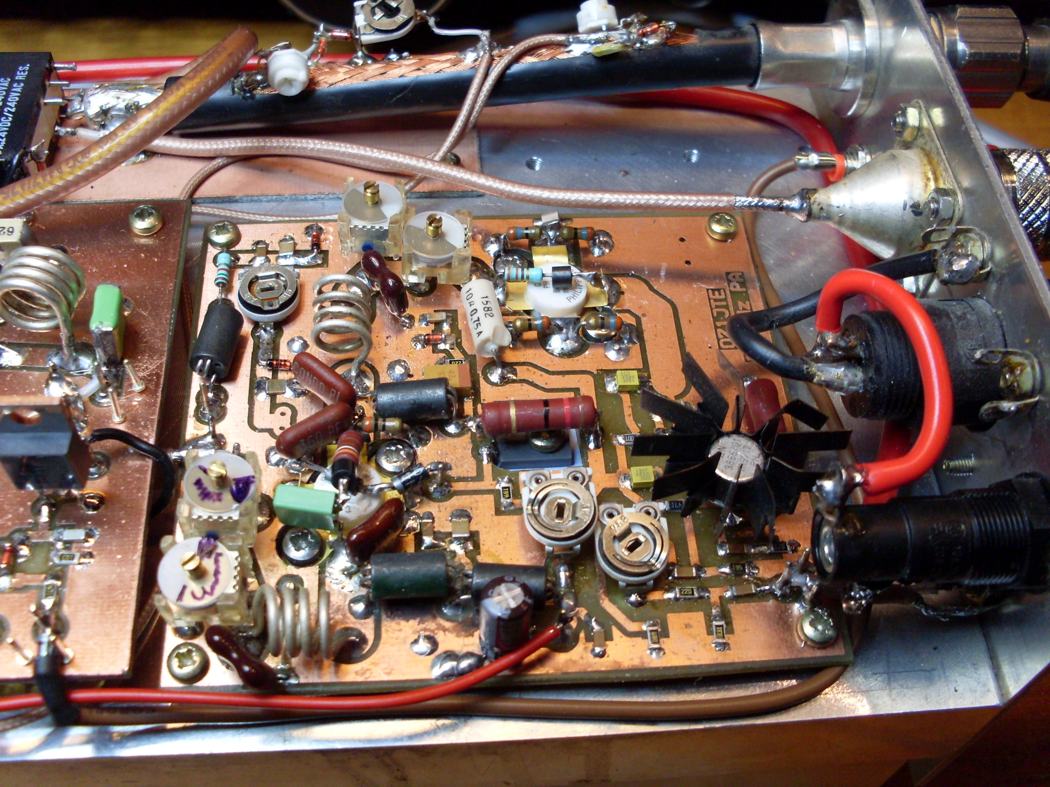
Fig. 7 Output PA |
Fig. 4 Output PA and at the top rear the ant. relay |
Low pass filter.
Although the push-pull design ensure that 2. harmonic is fairly depressed you can't underestimate the need of a low pass filter.
I designed a elliptic filter having 2 stop band, and I measured the loss to 0.25 dB so I was satisfied with this design.
On the low pass filter board I also build a fairly simple SWR protection and a PTT circuit that has a fault protection. I didn't make a real sequencer for the PTT as the amplifier maybe had deserved, just as the "power down protection" is a little brutal in the way I just take the power supply for the first (25 W) amplifier, but everything seems to work flawlessly the way it is.
The protection circuit is trigged by a voltage coming from the return port at directional coupler to the SCR gate.
The directional coupler is made by a piece of RG-213 coaxial cable where I have stitched 2 pieces of small wire underneath the outer wire braid. The small wire runs 40 mm underneath before it turns up again. In one end of these wires I placed a 47 Ohm resistor and the other end holds the detector diodes and a 10 nF capasitor.
One of the wires and belonging components is made in reverse so you have a "Forward" but also a "return" port now.
My coupler is producing just enough voltage on the return port to trigger the power down SCR at a SWR of 1:2.5.
If your SWR bridge has a higher output then you can modify R19 and R20 to adjust the trigger point.
In Fig. 3 You can rearmost just see the SWR bridge.
Put it together.
If you find a useful heat sink the rest of the assembly should be quite straight forward. I chose to make a little roof made of tin plate on top of the transistor package. Also make a good connection between the flange of the device to ground. Fig. 7 shows this detail. Always remember to make a lot of plate through holes to insure good RF grounding everywhere.
I hope my pictures will show most of the remaining details. As you can see some of the components are SMD and some are leaded so please check the part list for more details.
The detector diodes and belonging components are mounted directly on top of the RG-213 cable to form the SWR bridge.
One thing you can't see out of the schematic is that I have mounted another 24 V relay parallel to the antenna relay. This relay will ensure the power supply voltage for the first 25 W amplifier as well as the bias voltage for amplifier number 2 (120 W).
This is done to make the "power down" function work if the protection circuit sees a fault. This parallel relay will stop feeding 24 V to the first amplifier and the hole amplifier stop operating.
A better solution would have been to disable a input power relay, but this amplifier doesn't have a input relay, so this was an easy way to do it.
As you can see out of the shematic for the first amplifier, there is room for another bias circuit. This is done if you chose to replace the BJT transistor with a FET transistor. Then you need another kind of bias supply.
I made this option because i didn't knew if I needed more gain when I designed this stage. I found that the BLW50F gave me plenty of gain, so I had no need of the FET option after all.
Maybe you dont like my antenna relay, but my miniVNA tells me that return loss and insertion loss are pretty good (when I placed it laying and close to ground), so I found no need for a fancy and expansive solution.
My Results.
When I tested the amplifier it was clear to me that the low supply voltage was causing lower gain then normal for the devises. I could achieve approximately 5.8 dB gain.
But I found that just a little more supply voltage would give a very big different in gain and output power.
I chose to raise the power supply voltage to 28 V. This happens totally flawless and causes only a little more life in the amplifier.
At the end of my small testpins I only had 26,6 V and this now gave an output of 120 Watt when I feed the amplifier with the 25 W from the first stage. So as you can tell my gain is now 6.8 dB at the new power supply voltage. (Only a couple of volt).
The PA could give you a lot more watts, if you increase the input, but then the output transformer will limit the max. output. This is because of the combination of the 1:2 transformer and 28 V.
I decided to set the output for 120 Watt. The current draw is 7 Amp. An affectivity of 64 %. The complete amplifier draws 9.1 Amp.
What to improve?
Maybe the amplifier had deserved a real sequencer and also a more smooth power down sequence, and maybe also a fine coaxial relay, but everything seems to work flawlessly up to now, so I believe that it will stay that way.
Literature:
1. OZ1JTE Thomas ”QRP Booster” Danish radio magazine ”OZ” number. 4 2007. Danish languge.
2. OZ7TA Jørgens “Bredbånds HF PA-trin med transistorer” Danish radio magazine “OZ” Temahæfte 1990. Danish languge.